This website uses cookies. By using this site, you consent to the use of cookies. For more information, please take a look at our Privacy Policy.

F280039CPZRQ1 +BOM

2.8V~3.63V 120MHz 57 LQFP-100(14x14) Microcontroller Units (MCUs/MPUs/SOCs) ROHS

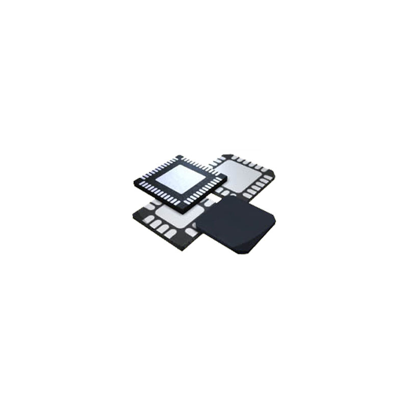
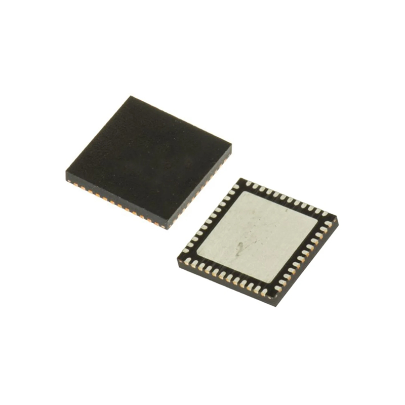
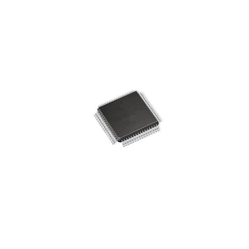
F280039CPZRQ1 General Description

The TMS320F28003x (F28003x) is a member of the C2000™ real-time microcontroller family of scalable, ultra-low latency devices designed for efficiency in power electronics, including but not limited to: high power density, high switching frequencies, and supporting the use of GaN and SiC technologies.

These include such applications as:

  • Motor drives
  • Appliances
  • Hybrid, electric & powertrain systems
  • Solar & EV charging
  • Digital power
  • Body electronics & lighting
  • Test & measurement

The real-time control subsystem is based on TI’s 32-bit C28x DSP core, which provides 120 MHz of signal-processing performance for floating- or fixed-point code running from either on-chip flash or SRAM. The C28x CPU is further boosted by the Floating-Point Unit (FPU), Trigonometric Math Unit (TMU), and VCRC (Cyclical Redundancy Check) extended instruction sets, speeding up common algorithms key to real-time control systems.

The CLA allows significant offloading of common tasks from the main C28x CPU. The CLA is an independent 32-bit floating-point math accelerator that executes in parallel with the CPU. Additionally, the CLA has its own dedicated memory resources and it can directly access the key peripherals that are required in a typical control system. Support of a subset of ANSI C is standard, as are key features like hardware breakpoints and hardware task-switching.

The F28003x supports up to 384KB (192KW) of flash memory divided into three 128KB (64KW) banks, which enable programming and execution in parallel. Up to 69KB (34.5KW) of on-chip SRAM is also available to supplement the flash memory.

The Live Firmware Update hardware enhancements on F28003x allow fast context switching from the old firmware to the new firmware to minimize application downtime when updating the device firmware.

High-performance analog blocks are integrated on the F28003x real-time microcontroller (MCU) and are closely coupled with the processing and PWM units to provide optimal real-time signal chain performance. Sixteen PWM channels, all supporting frequency-independent resolution modes, enable control of various power stages from a 3-phase inverter to power factor correction and advanced multilevel power topologies.

The inclusion of the Configurable Logic Block (CLB) allows the user to add custom logic and potentially integrate FPGA-like functions into the C2000 real-time MCU.

Interfacing is supported through various industry-standard communication ports (such as SPI, SCI, I2C, PMBus, LIN, CAN and CAN FD) and offers multiple pin-muxing options for optimal signal placement. The Fast Serial Interface (FSI) enables up to 200Mbps of robust communications across an isolation boundary.

New to the C2000 platform is the Host Interface Controller (HIC), a high-throughput interface that allows an external host to access the resources of the TMS320F28003x directly.

Want to learn more about features that make C2000 Real-Time MCUs the right choice for your real-time control system? Check out The Essential Guide for Developing With C2000™ Real-Time Microcontrollers and visit the C2000™ real-time control MCUs page.

The Getting Started With C2000™ Real-Time Control Microcontrollers (MCUs) Getting Started Guide covers all aspects of development with C2000 devices from hardware to support resources. In addition to key reference documents, each section provides relevant links and resources to further expand on the information covered.

Ready to get started? Check out the TMDSCNCD280039C evaluation board and download C2000Ware.

Key Features

  • TMS320C28x 32-bit DSP core at 120 MHz
    • IEEE 754 Floating-Point Unit (FPU)
      • Support for Fast Integer Division (FINTDIV)
    • Trigonometric Math Unit (TMU)
      • Support for Nonlinear Proportional Integral Derivative (NLPID) control
    • CRC Engine and Instructions (VCRC)
    • Ten hardware breakpoints (with ERAD)
  • Programmable Control Law Accelerator (CLA)
    • 120 MHz
    • IEEE 754 single-precision floating-point instructions
    • Executes code independently of main CPU
  • On-chip memory
    • 384KB (192KW) of flash (ECC-protected) across three independent banks
    • 69KB (34.5KW) of RAM (ECC-protected)
    • Dual-zone security
    • Secure Boot and JTAG Lock
  • Clock and system control
    • Two internal 10-MHz oscillators
    • Crystal oscillator or external clock input
    • Windowed watchdog timer module
    • Missing clock detection circuitry
    • Dual-clock Comparator (DCC)
  • 3.3-V I/O design
    • Internal VREG generation allows for single-supply design
    • Brownout reset (BOR) circuit
  • System peripherals
    • 6-channel Direct Memory Access (DMA) controller
    • 55 individually programmable multiplexed General-Purpose Input/Output (GPIO) pins
    • 23 digital inputs on analog pins
    • 2 digital inputs/outputs on analog pins (AGPIO)
    • Enhanced Peripheral Interrupt Expansion (ePIE)
    • Multiple low-power mode (LPM) support
    • Embedded Real-time Analysis and Diagnostic (ERAD)
    • Unique Identification (UID) number
  • Communications peripherals
    • One Power-Management Bus (PMBus) interface
    • Two Inter-integrated Circuit (I2C) interfaces
    • One Controller Area Network (CAN/DCAN) bus port
    • One Controller Area Network with Flexible Data-Rate (CAN FD/MCAN) bus port
    • Two Serial Peripheral Interface (SPI) ports
    • Two UART-compatible Serial Communication Interface (SCI)
    • Two UART-compatible Local Interconnect Network (LIN) interfaces
    • Fast Serial Interface (FSI) with one transmitter and one receiver (up to 200Mbps)
  • Analog system
    • Three 4-MSPS, 12-bit Analog-to-Digital Converters (ADCs)
      • Up to 23 external channels (includes the two gpdac outputs)
      • Four integrated Post-Processing Blocks (PPB) per ADC
    • Four windowed comparators (CMPSS) with 12-bit reference Digital-to-Analog Converters (DACs)
      • Digital glitch filters
    • Two 12-bit buffered DAC outputs
  • Enhanced control peripherals
    • 16 ePWM channels with eight channels that have high-resolution capability (150-ps resolution)
      • Integrated dead-band support
      • Integrated hardware trip zones (TZs)
    • Three Enhanced Capture (eCAP) modules
      • High-resolution Capture (HRCAP) available on one of the three eCAP modules
    • Two Enhanced Quadrature Encoder Pulse (eQEP) modules with support for CW/CCW operation modes
    • Eight Sigma-Delta Filter Module (SDFM) input channels (two parallel filters per channel)
      • Standard SDFM data filtering
      • Comparator filter for fast action for overvalue or undervalue condition
    • Embedded Pattern Generator (EPG)
  • Configurable Logic Block (CLB)
    • 4 tiles
    • Augments existing peripheral capability
    • Supports position manager solutions
  • Host Interface Controller (HIC)
    • Access to internal memory from an external host
  • Background CRC (BGCRC)
    • One cycle CRC computation on 32 bits of data
  • Advanced Encryption Standard (AES) accelerator
  • Live Firmware Update (LFU)
    • Fast context switching from old to new firmware
    • Flash bank erase time improvements
  • Diagnostic features
    • Memory Power On Self Test (MPOST)
    • Hardware Built-in Self Test (HWBIST)
  • Functional Safety-Compliant targeted
    • Developed for functional safety applications

    • Documentation available to aid ISO 26262 and IEC 61508 system design

    • Systematic capability up to ASIL D and SIL 3 targeted

    • Hardware capability up to ASIL B and SIL 2 targeted

  • Safety-related certification
    • ISO 26262 certification up to ASIL B and SIL 2 by TÜV SÜD planned

  • Package options:
    • 100-pin Low-profile Quad Flatpack (LQFP) [PZ suffix]
    • 80-pin Low-profile Quad Flatpack (LQFP) [PN suffix]
    • 64-pin (LQFP) [PM suffix]
    • 48-pin (LQFP) [PT suffix]
  • Temperature options:
    • Free-air (TA): –40°C to 125°C
    • Junction (TJ): –40°C to 150°C

Specifications

CPU C28x, CLA Frequency (MHz) 120
Flash memory (kByte) 384 RAM (kByte) 69
ADC resolution (Bps) 12 Total processing (MIPS) 240
Features CAN FD, Configurable logic block, Dual security zones, FPU32 UART 4
CAN (#) 2 Sigma-delta filter 8
PWM (Ch) 16 TI functional safety category Functional Safety-Compliant
Number of ADC channels 14, 16, 18, 23 Direct memory access (Ch) 6
SPI 2 QEP 2
USB No Operating temperature range (°C) -40 to 125
Rating Automotive Communication interface CAN, CAN FD, FSI, I2C, LIN, PMBUS, SCI, SPI, UART

Service Policies and Others

After-Sales & Settlement Related

payment Payment

Payment Method

hsbc
TT/Wire Transfer
paypal
Paypal
wu
Western Union
mg
Money Gram

For alternative payment channels, please reach out to us at:

[email protected]
shipping Shipping & Packing

Shipping Method

fedex
Fedex
ups
UPS
dhl
DHL
tnt
NTN
Packing

AVAQ determines and packages all devices based on electrostatic discharge (ESD) and moisture sensitivity level (MSL) protection requirements.

Warranty Warranty

We promise to provide 365 days quality assurance service for all our products.

Reviews

You need to log in to reply. Sign In | Sign Up

In Stock: 7,072

Minimum Order: 1

Qty. Unit Price Ext. Price
1+ - -

The prices below are for reference only.