Payment Method


LDO Regulator, 1 A, Fixed and Adjustable, Positive
Manufacturer:
Mfr.Part #:
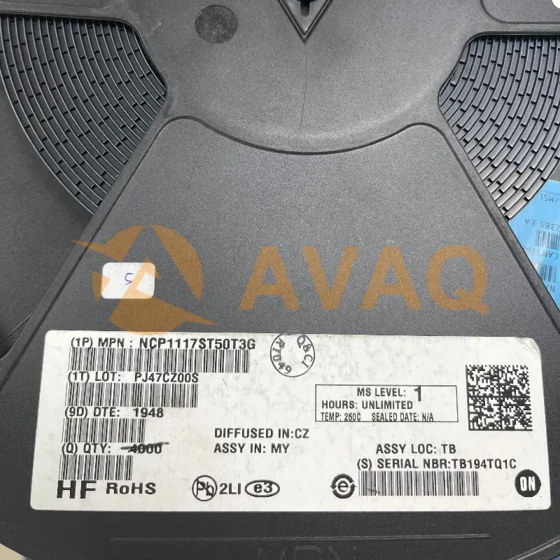
NCP1117ST50T3G
Datasheet:
Output Configuration:
Positive
Output Type:
Fixed
Number of Regulators:
1
Voltage - Input (Max):
20V
EDA/CAD Models:
Please fill in the short form below and we will provide you the quotation immediately.
The NCP1117 series comprises low dropout (LDO) positive linear voltage regulators capable of delivering an output current exceeding 1.0 A. They exhibit a maximum dropout voltage of 1.2 V when supplying 800 mA, even across a range of temperatures. This series includes eight fixed output voltage options: 1.5 V, 1.8 V, 2.0 V, 2.5 V, 2.85 V, 3.3 V, 5.0 V, and 12 V, all of which maintain regulation without needing a minimum load.
Additionally, there's an adjustable output version that can be set between 1.25 V and 18.8 V using two external resistors. The on-chip trimming ensures the reference/output voltage accuracy within +/- 1.0%. These regulators incorporate internal protection mechanisms, such as output current limiting, safe operating area compensation, and thermal shutdown.
The NCP1117 series can handle input voltages of up to 20 V. These devices are available in SOT223 and DPAK packages.
How NCP1117ST50T3G Work?
The NCP1117ST50T3G operates as a low-drop positive voltage regulator, commonly employed in switching power supply circuits to deliver a consistent and stable 5V output. A typical application of the NCP1117ST50T3G is in a full-wave diode rectifier power supply circuit. In this setup, there are three key stages:
Power Transformer: This is the first stage of the circuit, and its role is to step down the high-voltage AC input (usually 220V or 120V AC) to a lower AC voltage, typically 5V AC.
Diode Rectifier: The second stage of the circuit is the diode rectifier. It takes the 5V AC output from the transformer and converts it into a 5V DC output. This conversion involves converting the alternating current (AC) into direct current (DC).
LD1117 Regulator: The third and final stage is where the NCP1117ST50T3G voltage regulator, often referred to as LD1117, comes into play. Its primary function is to smooth out any remaining ripple or fluctuations in the converted DC voltage from the diode rectifier. The LD1117 ensures that the output voltage is stable and remains at a constant 5V DC.
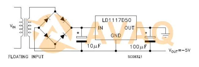
How NCP1117ST50T3G Work
NCP1117 Pinout
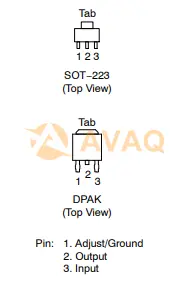
NCP1117 Pinout
Specifications
Features
NCP1117ST50T3G Alternatives
NCP1117ST50T3G Datasheet PDF
Check and Download NCP1117ST50T3G Datasheet PDF here>>
| Category | Integrated Circuits (ICs)Power Management (PMIC)Voltage Regulators - Linear | Series | - |
| Output Configuration | Positive | Output Type | Fixed |
| Number of Regulators | 1 | Voltage - Input (Max) | 20V |
| Voltage - Output (Min/Fixed) | 5V | Voltage - Output (Max) | - |
| Voltage Dropout (Max) | 1.2V @ 800mA | Current - Output | 1A |
| Current - Quiescent (Iq) | 10 mA | PSRR | 61dB (120Hz) |
| Control Features | - | Protection Features | Over Current, Over Temperature |
| Operating Temperature | 0°C ~ 125°C | Mounting Type | Surface Mount |
| Base Product Number | NCP1117 |
After-Sales & Settlement Related
 Payment
Payment Method


For alternative payment channels, please reach out to us at:
[email protected] Shipping & Packing
Shipping Method


AVAQ determines and packages all devices based on electrostatic discharge (ESD) and moisture sensitivity level (MSL) protection requirements.
 Warranty

365-Day Product
Quality Guarantee
We promise to provide 365 days quality assurance service for all our products.
| Qty. | Unit Price | Ext. Price |
|---|---|---|
| 1+ | - | - |
The prices below are for reference only.
All bill of materials (BOM) can be sent via email to ![]() [email protected],
or fill below form to Quote for NCP1117ST50T3G, guaranteed quotes back within
[email protected],
or fill below form to Quote for NCP1117ST50T3G, guaranteed quotes back within
![]() 12hr.
12hr.

Item as described. Packaging could be better and flux was not cleaned from the board, but everything works.