This website uses cookies. By using this site, you consent to the use of cookies. For more information, please take a look at our Privacy Policy.

TLC272CDR

Dual, 16-V, 2-MHz, In to V- operational amplifier

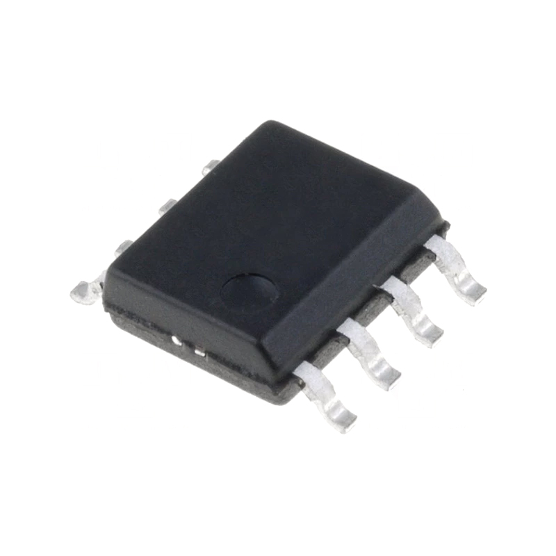
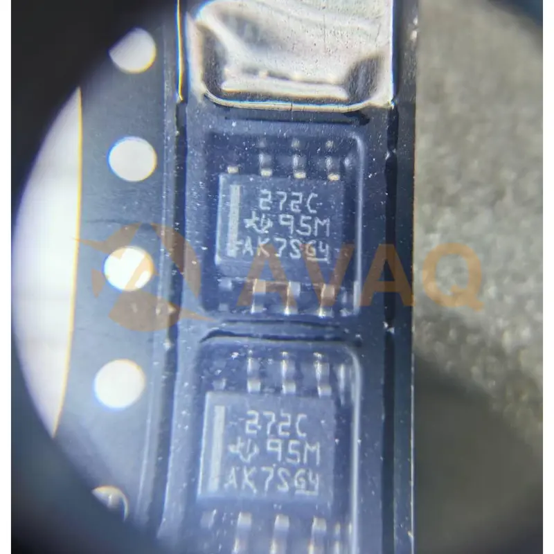
TLC272CDR General Description

The TLC272 and TLC277 precision dual operational amplifiers combine a wide range of input offset voltage grades with low offset voltage drift, high input impedance, low noise, and speeds approaching those of general-purpose BiFET devices.

These devices use Texas Instruments silicon-gate LinCMOS™ technology, which provides offset voltage stability far exceeding the stability available with conventional metal-gate processes.

The extremely high input impedance, low bias currents, and high slew rates make these cost-effective devices ideal for applications previously reserved for BiFET and NFET products. Four offset voltage grades are available (C-suffix and I-suffix types), ranging from the low-cost TLC272 (10 mV) to the high-precision TLC277 (500 uV). These advantages, in combination with good common-mode rejection and supply voltage rejection, make these devices a good choice for new state-of-the-art designs as well as for upgrading existing designs.

In general, many features associated with bipolar technology are available on LinCMOS™ operational amplifiers without the power penalties of bipolar technology. General applications such as transducer interfacing, analog calculations, amplifier blocks, active filters, and signal buffering are easily designed with the TLC272 and TLC277. The devices also exhibit low voltage single-supply operation, making them ideally suited for remote and inaccessible battery-powered applications. The common-mode input voltage range includes the negative rail.

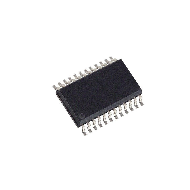
A wide range of packaging options is available, including small-outline and chip carrier versions for high-density system applications.

The device inputs and outputs are designed to withstand –100-mA surge currents without sustaining latch-up.

The TLC272 and TLC277 incorporate internal ESD-protection circuits that prevent functional failures at voltages up to 2000 V as tested under MIL-STD-883C, Method 3015.2; however, care should be exercised in handling these devices as exposure to ESD may result in the degradation of the device parametric performance.

The C-suffix devices are characterized for operation from 0°C to 70°C. The I-suffix devices are characterized for operation from –40°C to 85°C. The M-suffix devices are characterized for operation over the full military temperature range of –55°C to 125°C.

Key Features

  • Trimmed Offset Voltage:
    TLC277 . . . 500 uV Max at 25°C, VDD = 5 V
  • Input Offset Voltage Drift .Typically 0.1 uV/Month, Including the First 30 Days
  • Wide Range of Supply Voltages Over Specified Temperature Range:
    0°C to 70°C .3 V to 16 V
    –40°C to 85°C .4 V to 16 V
    –55°C to 125°C .4 V to 16 V
  • Single-Supply Operation
  • Common-Mode Input Voltage Range Extends Below the Negative Rail (C-Suffix, I-Suffix types)
  • Low Noise .Typically 25 nV/Hz at f = 1 kHz
  • Output Voltage Range Includes Negative Rail
  • High Input impedance .1012 Typ
  • ESD-Protection Circuitry
  • Small-Outline Package Option Also Available in Tape and Reel
  • Designed-In Latch-Up Immunity

LinCMOS is a trademark of Texas Instruments.

Application

  • Industrial

Specifications

Number of channels 2 Total supply voltage (+5 V = 5, ±5 V = 10) (max) (V) 16
Total supply voltage (+5 V = 5, ±5 V = 10) (min) (V) 3 Rail-to-rail In to V-
GBW (typ) (MHz) 2 Slew rate (typ) (V/µs) 3.6
Vos (offset voltage at 25°C) (max) (mV) 10 Iq per channel (typ) (mA) 0.7
Vn at 1 kHz (typ) (nV√Hz) 25 Rating Catalog
Operating temperature range (°C) -40 to 85, 0 to 70 Offset drift (typ) (µV/°C) 1.8
Input bias current (max) (pA) 60 CMRR (typ) (dB) 80
Iout (typ) (A) 0.01 Architecture CMOS
Input common mode headroom (to negative supply) (typ) (V) -0.3 Input common mode headroom (to positive supply) (typ) (V) -0.8
Output swing headroom (to negative supply) (typ) (V) 0.03 Output swing headroom (to positive supply) (typ) (V) -1.2

Service Policies and Others

After-Sales & Settlement Related

payment Payment

Payment Method

hsbc
TT/Wire Transfer
paypal
Paypal
wu
Western Union
mg
Money Gram

For alternative payment channels, please reach out to us at:

[email protected]
shipping Shipping & Packing

Shipping Method

fedex
Fedex
ups
UPS
dhl
DHL
tnt
NTN
Packing

AVAQ determines and packages all devices based on electrostatic discharge (ESD) and moisture sensitivity level (MSL) protection requirements.

Warranty Warranty

We promise to provide 365 days quality assurance service for all our products.

Reviews

You need to log in to reply. Sign In | Sign Up

Availability: 7255 PCS

+BOM
Qty. Unit Price Ext. Price
1+ $0.447 $0.45
10+ $0.357 $3.57
30+ $0.318 $9.54
100+ $0.271 $27.10
500+ $0.248 $124.00
1000+ $0.235 $235.00

The prices below are for reference only.