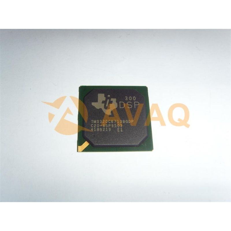
V62/07649-02XA General Description
The C64x+™ DSPs (including the SM320C6455-EP device) are the highest-performance fixed-point DSP generation in the C6000™ DSP platform. The C6455 device is based on the third-generation high-performance, advanced VelociTI™ very-long-instruction-word (VLIW) architecture developed by Texas Instruments (TI), making these DSPs an excellent choice for applications including video and telecom infrastructure, imaging/medical, and wireless infrastructure (WI). The C64x+™ devices are upward code-compatible from previous devices that are part of the C6000™ DSP platform.
Based on 90-nm process technology and with performance of up to 9600 million instructions per second (MIPS) [or 9600 16 bit MMACs per cycle] at a 1.2-GHz clock rate, the C6455 device offers cost-effective solutions to high-performance DSP programming challenges. The C6455 DSP possesses the operational flexibility of high-speed controllers and the numerical capability of array processors.
The C64x+ DSP core employs eight functional units, two register files, and two data paths. Like the earlier C6000 devices, two of these eight functional units are multipliers or .M units. Each C64x+ .M unit doubles the multiply throughput versus the C64x core by performing four 16 bit x 16 bit multiply-accumulates (MACs) every clock cycle. Thus, eight 16 bit x 16 bit MACs can be executed every cycle on the C64x+ core. At a 1.2-GHz clock rate, this means 9600 16 bit MMACs can occur every second. Moreover, each multiplier on the C64x+ core can compute one 32 bit x 32 bit MAC or four 8 bit x 8 bit MACs every clock cycle.
The C6455 device includes Serial RapidIO. This high bandwidth peripheral dramatically improves system performance and reduces system cost for applications that include multiple DSPs on a board, such as video and telecom infrastructures and medical/imaging.
The C6455 DSP integrates a large amount of on-chip memory organized as a two-level memory system. The level-1 (L1) program and data memories on the C6455 device are 32KB each. This memory can be configured as mapped RAM, cache, or some combination of the two. When configured as cache, L1 program (L1P) is a direct mapped cache where as L1 data (L1D) is a two-way set associative cache. The level 2 (L2) memory is shared between program and data space and is 2096KB in size. L2 memory also can be configured as mapped RAM, cache, or some combination of the two. The C64x+ Megamodule also has a 32 bit peripheral configuration (CFG) port, an internal DMA (IDMA) controller, a system component with reset/boot control, interrupt/exception control, a power-down control, and a free-running 32 bit timer for time stamp.
The peripheral set includes: an inter-integrated circuit bus module (I2C); two multichannel buffered serial ports (McBSPs); an 8 bit Universal Test and Operations PHY Interface for Asynchronous Transfer Mode (ATM) Slave [UTOPIA Slave] port; two 64 bit general-purpose timers (also configurable as four 32 bit timers); a user-configurable 16 bit or 32 bit host-port interface (HPI16/HPI32); a peripheral component interconnect (PCI); a 16-pin general-purpose input/output port (GPIO) with programmable interrupt/event generation modes; an 10/100/1000 Ethernet media access controller (EMAC), which provides an efficient interface between the C6455 DSP core processor and the network; a management data input/output (MDIO) module (also part of the EMAC) that continuously polls all 32 MDIO addresses in order to enumerate all PHY devices in the system; a glueless external memory interface (64 bit EMIFA), which is capable of interfacing to synchronous and asynchronous peripherals; and a 32 bit DDR2 SDRAM interface.
The I2C ports on the C6455 allow the DSP to easily control peripheral devices and communicate with a host processor. In addition, the standard multichannel buffered serial port (McBSP) may be used to communicate with serial peripheral interface (SPI) mode peripheral devices.
The C6455 device has two high-performance embedded coprocessors [enhanced Viterbi Decoder Coprocessor (VCP2) and enhanced Turbo Decoder Coprocessor (TCP2)] that significantly speed up channel-decoding operations on-chip. The VCP2 operating at CPU clock divided-by-3 can decode over 694 7.95-Kbps adaptive multi-rate (AMR) [K = 9, R = 1/3] voice channels. The VCP2 supports constraint lengths K = 5, 6, 7, 8, and 9, rates R = 3/4, 1/2, 1/3, 1/4, and 1/5 and flexible polynomials, while generating hard decisions or soft decisions. The TCP2 operating at CPU clock divided-by-3 can decode up to fifty 384-Kbps or eight 2-Mbps turbo encoded channels (assuming 6 iterations). The TCP2 implements the max*log-map algorithm and is designed to support all polynomials and rates required by Third-Generation Partnership Projects (3GPP and 3GPP2), with fully programmable frame length and turbo interleaver. Decoding parameters such as the number of iterations and stopping criteria are also programmable. Communications between the VCP2/TCP2 and the CPU are carried out through the EDMA3 controller.
The C6455 has a complete set of development tools which includes: a new C compiler, an assembly optimizer to simplify programming and scheduling, and a Windows® debugger interface for visibility into source code execution.
Key Features
- Controlled Baseline
- One Assembly Site
- Test Site
- One Fabrication Site
- Enhanced Diminishing Manufacturing Sources (DMS) Support
- Enhanced Product-Change Notification
- Qualification Pedigree(1)
- High-Performance Fixed-Point DSP (C6455)
- 1.39 ns, 1.17 ns, 1 ns, and 0.83 ns Instruction Cycle Time
- 1 GHz Clock Rate
- Eight 32 Bit Instructions/Cycle
- 9600 MIPS/MMACS (16 Bits)
- Commercial Temperature (0°C to 90°C)
- Extended Temperature (-40°C to 105°C)
- S-Temp (-55°C to 105°C)
- C64x+™ DSP Core
- Dedicated SPLOOP Instruction
- Compact Instructions (16 Bit)
- Instruction Set Enhancements
- Exception Handling
- C64x+ Megamodule L1/L2 Memory Architecture:
- 256K Bit (32K Byte) L1P Program Cache Direct Mapped)
- 256K Bit (32K Byte) L1D Data Cache 2-Way Set-Associative]
- 16M Bit (2096K Byte) L2 Unified Mapped RAM/Cache (Flexible Allocation)
- 256K Bit (32K Byte) L2 ROM
- Time Stamp Counter
- Enhanced VCP2
- Supports Over 694 7.95 Kbps AMR
- Programmable Code Parameters
- Enhanced Turbo Decoder Coprocessor (TCP2)
- Supports up to Eight 2 Mbps 3GPP (6 Iterations)
- Programmable Turbo Code and Decoding Parameters
- Endianess: Little Endian, Big Endian
- 64 Bit External Memory Interface (EMIFA)
- Glueless Interface to Asynchronous Memories (SRAM, Flash, and EEPROM) and Synchronous Memories (SBSRAM, ZBT SRAM)
- Supports Interface to Standard Sync Devices and Custom Logic (FPGA, CPLD, ASICs, etc.)
- 32M Byte Total Addressable External Memory Space
- Four 1x Serial RapidIO® Links (or One 4x), v1.2 Compliant
- 1.25/2.5/3.125 Gbps Link Rates
- Message Passing, DirectIO Support, Error Management Extensions, and Congestion Control
- IEEE 1149.6 Compliant I/Os
- DDR2 Memory Controller
- Interfaces to DDR2-533 SDRAM
- 32 Bit/16 Bit, 533 MHz (data rate) Bus
- 512M Byte Total Addressable External Memory Space
- EDMA3 Controller (64 Independent Channels)
- 32/16 Bit Host-Port Interface (HPI)
- 32 Bit 33/66 MHz, 3.3 V Peripheral Component Interconnect (PCI) Master/Slave Interface Conforms to PCI Local Bus Specification version 2.3)
- One InterIntegrated Circuit (I2C) Bus
- Two McBSPs
- 10/100/1000 Mb/s Ethernet MAC (EMAC)
- IEEE 802.3 Compliant
- Supports Multiple Media Independent Interfaces (MII, GMII, RMII, and RGMII)
- Eight Independent Transmit (TX) and Eight Independent Receive (RX) Channels
- Two 64 Bit General-Purpose Timers, Configurable as Four 32 Bit Timers
- UTOPIA
- UTOPIA Level 2 Slave ATM Controller
- 8 Bit Transmit and Receive Operations up to 50 MHz per Direction
- User-Defined Cell Format up to 64 Bytes
- 16 General-Purpose I/O (GPIO) Pins
- System PLL and PLL Controller
- Secondary PLL and PLL Controller, Dedicated to EMAC and DDR2 Memory Controller
- Advanced Event Triggering (AET) Compatible
- Trace-Enabled Device
- IEEE-1149.1 (JTAG™) Boundary-Scan-Compatible
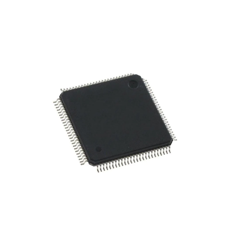
- 697-Pin Ball Grid Array (BGA) Package ZTZ or GTZ Suffix), 0.8 mm Ball Pitch
- 0.09 µm/7-Level Cu Metal Process (CMOS)
- 3.3/1.8/1.5/1.25/1.2 V I/Os, 1.25/1.2 V Internal
(1)Component qualification in accordance with JEDEC and industry standards to ensure reliable operation over an extended temperature range. This includes, but is not limited to, Highly Accelerated Stress Test (HAST) or biased 85/85, temperature cycle, autoclave or unbiased HAST, electromigration, bond intermetallic life, and mold compound life. Such qualification testing should not be viewed as justifying use of this component beyond specified performance and environmental limits.
C64x+, JTAG, C64x+, VelociTI, C6000, Code Composer Studio, DSP/BIOS, XDS are trademarks of Texas Instruments.

 Payment


 Shipping & Packing


 Warranty