Payment Method


231MHz 130nm Technology
208-BFQFPManufacturer:
Microchip Technology
Mfr.Part #:
A3P1000-PQ208
Datasheet:
Series:
ProASIC3
Programmabe:
Not Verified
Total RAM Bits:
147456
Number Of I/O:
154
EDA/CAD Models:
Send all BOMs to ![]() [email protected],
or fill out the form below for a quote on A3P1000-PQ208. Guaranteed response within
[email protected],
or fill out the form below for a quote on A3P1000-PQ208. Guaranteed response within
![]() 12hr.
12hr.
Please fill in the short form below and we will provide you the quotation immediately.
The A3P1000-PQ208 FPGA by Microsemi is a cutting-edge solution for digital signal processing, image processing, and communication protocols. With its 100,000 logic elements and 2880 kilobits of memory, this FPGA offers high logic density and memory capacity for complex applications. The device's plastic quad flat pack (PQ208) package provides ease of soldering and handling during assembly, and its 1.2V operating voltage makes it energy-efficient for battery-operated applications. Additionally, the FPGA supports a wide range of functions and can be easily programmed using Microsemi's Libero SoC software, making it a versatile and user-friendly choice for FPGA design and implementation
| Series | ProASIC3 | Programmabe | Not Verified |
| Total RAM Bits | 147456 | Number of I/O | 154 |
| Number of Gates | 1000000 | Voltage - Supply | 1.425V ~ 1.575V |
| Mounting Type | Surface Mount | Operating Temperature | 0°C ~ 85°C (TJ) |
| Base Product Number | A3P1000 |
After-Sales & Settlement Related
 Payment
Payment Method


For alternative payment channels, please reach out to us at:
[email protected] Shipping & Packing
Shipping Method


AVAQ determines and packages all devices based on electrostatic discharge (ESD) and moisture sensitivity level (MSL) protection requirements.
 Warranty

365-Day Product
Quality Guarantee
We promise to provide 365 days quality assurance service for all our products.
| Qty. | Unit Price | Ext. Price |
|---|---|---|
| 1+ | - | - |
The prices below are for reference only.

NE555
Texas Instruments
100kHz operation frequency with low power consumption for long-lasting performance

CD4017
Onsemi
Compact digital counter for precision measurement application

74LS04
Onsemi
High-quality die for professional use only, unsurfaced and untested

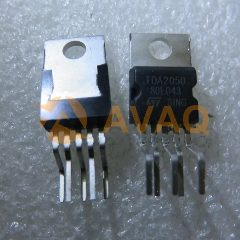
TDA2050
Stmicroelectronics
Effortlessly drives your speakers with crystal-clear sound and robust power

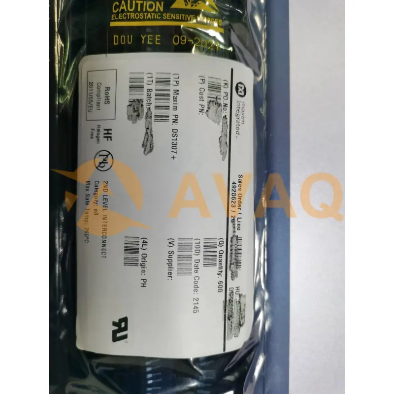
DS1307+
Analog Devices
I2C DIP-8 Real-time Clocks (RTC) ROHS