Payment Method


Packaged in a 100-pin VQFP tray for easy integration into electronic systems
VQFP-100Manufacturer:
MICROCHIP TECHNOLOGY INC
Mfr.Part #:
A3P250-VQG100T
Datasheet:
Part Life Cycle Code:
Active
Reach Compliance Code:
compliant
HTS Code:
8542.39.00.01
Factory Lead Time:
52 Weeks
Send all BOMs to ![]() [email protected],
or fill out the form below for a quote on A3P250-VQG100T. Guaranteed response within
[email protected],
or fill out the form below for a quote on A3P250-VQG100T. Guaranteed response within
![]() 12hr.
12hr.
Please fill in the short form below and we will provide you the quotation immediately.
Featuring a high-performance ARM Cortex-M3 processor, secure boot capabilities, and AES encryption, the A3P250-VQG100T FPGA prioritizes security and efficiency in its design. These advanced features ensure that sensitive data and operations are protected, making it an attractive option for applications where security is paramount. With its comprehensive feature set and powerful processing capabilities, the A3P250-VQG100T is poised to deliver exceptional performance in demanding applications
| Part Life Cycle Code | Active | Reach Compliance Code | compliant |
| HTS Code | 8542.39.00.01 | Factory Lead Time | 52 Weeks |
| Clock Frequency-Max | 350 MHz | JESD-30 Code | S-PQFP-G100 |
| JESD-609 Code | e3 | Length | 14 mm |
| Moisture Sensitivity Level | 3 | Number of CLBs | 6144 |
| Number of Equivalent Gates | 250000 | Number of Inputs | 68 |
| Number of Logic Cells | 6144 | Number of Outputs | 68 |
| Number of Terminals | 100 | Operating Temperature-Max | 125 °C |
| Operating Temperature-Min | -40 °C | Organization | 6144 CLBS, 250000 GATES |
| Peak Reflow Temperature (Cel) | 260 | Power Supplies | 1.5/3.3 V |
| Programmable Logic Type | FIELD PROGRAMMABLE GATE ARRAY | Qualification Status | Not Qualified |
| Screening Level | AEC-Q100 | Seated Height-Max | 1.2 mm |
| Supply Voltage-Max | 1.575 V | Supply Voltage-Min | 1.425 V |
| Supply Voltage-Nom | 1.5 V | Surface Mount | YES |
| Technology | CMOS | Temperature Grade | AUTOMOTIVE |
| Terminal Finish | MATTE TIN | Terminal Form | GULL WING |
| Terminal Pitch | 0.5 mm | Terminal Position | QUAD |
| Time@Peak Reflow Temperature-Max (s) | 30 | Width | 14 mm |
After-Sales & Settlement Related
 Payment
Payment Method


For alternative payment channels, please reach out to us at:
[email protected] Shipping & Packing
Shipping Method


AVAQ determines and packages all devices based on electrostatic discharge (ESD) and moisture sensitivity level (MSL) protection requirements.
 Warranty

365-Day Product
Quality Guarantee
We promise to provide 365 days quality assurance service for all our products.
| Qty. | Unit Price | Ext. Price |
|---|---|---|
| 1+ | - | - |
The prices below are for reference only.

NE555
Texas Instruments
100kHz operation frequency with low power consumption for long-lasting performance

CD4017
Onsemi
Compact digital counter for precision measurement application

74LS04
Onsemi
High-quality die for professional use only, unsurfaced and untested

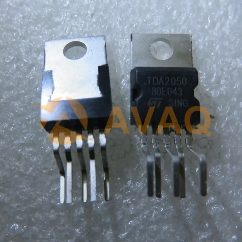
TDA2050
Stmicroelectronics
Effortlessly drives your speakers with crystal-clear sound and robust power

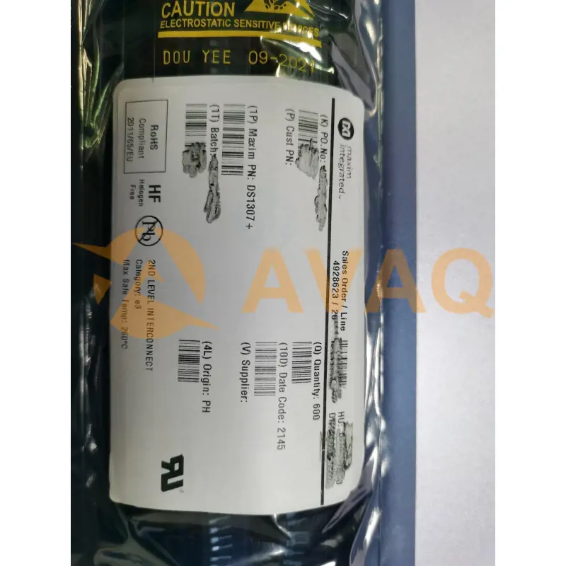
DS1307+
Analog Devices
I2C DIP-8 Real-time Clocks (RTC) ROHS