Payment Method


20V N & P Channel PowerTrench® MOSFETs
SC-70Manufacturer:
Mfr.Part #:
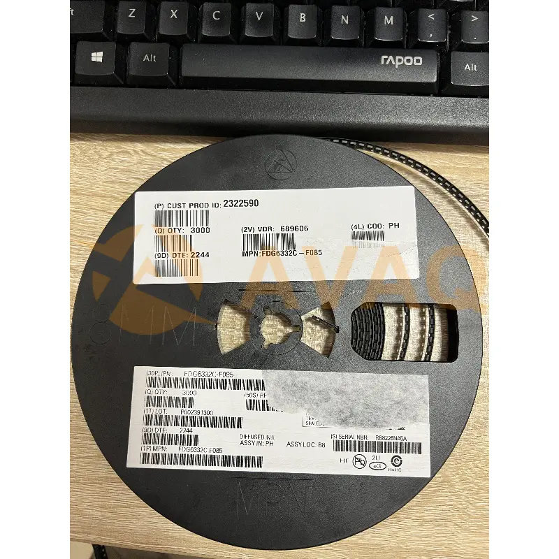
FDG6332C-F085
Datasheet:
Pbfree Code:
Yes
Part Life Cycle Code:
End Of Life
Reach Compliance Code:
compliant
ECCN Code:
EAR99
EDA/CAD Models:
Send all BOMs to ![]() [email protected],
or fill out the form below for a quote on FDG6332C-F085. Guaranteed response within
[email protected],
or fill out the form below for a quote on FDG6332C-F085. Guaranteed response within
![]() 12hr.
12hr.
Please fill in the short form below and we will provide you the quotation immediately.
The N & P-Channel MOSFETs are produced using an advanced PowerTrench process that has been especially tailored to minimize on-state resistance and yet maintain superior switching performance.These devices have been designed to offer exceptional power dissipation in a very small footprint for applications where the bigger more expensive TSSOP-8 and SSOP-6 packages are impractical.
| Source Content uid | FDG6332C-F085 | Pbfree Code | Yes |
| Part Life Cycle Code | End Of Life | Reach Compliance Code | compliant |
| ECCN Code | EAR99 | Configuration | SEPARATE, 2 ELEMENTS WITH BUILT-IN DIODE |
| DS Breakdown Voltage-Min | 20 V | Drain Current-Max (ID) | 0.7 A |
| Drain-source On Resistance-Max | 0.3 Ω | FET Technology | METAL-OXIDE SEMICONDUCTOR |
| JESD-30 Code | R-PDSO-G6 | JESD-609 Code | e3 |
| Moisture Sensitivity Level | 1 | Number of Elements | 2 |
| Number of Terminals | 6 | Operating Mode | ENHANCEMENT MODE |
| Operating Temperature-Max | 150 °C | Peak Reflow Temperature (Cel) | 260 |
| Polarity/Channel Type | N-CHANNEL AND P-CHANNEL | Power Dissipation-Max (Abs) | 0.3 W |
| Qualification Status | Not Qualified | Surface Mount | YES |
| Terminal Finish | MATTE TIN | Terminal Form | GULL WING |
| Terminal Position | DUAL | Time@Peak Reflow Temperature-Max (s) | 30 |
| Transistor Application | SWITCHING | Transistor Element Material | SILICON |
After-Sales & Settlement Related
 Payment
Payment Method


For alternative payment channels, please reach out to us at:
[email protected] Shipping & Packing
Shipping Method


AVAQ determines and packages all devices based on electrostatic discharge (ESD) and moisture sensitivity level (MSL) protection requirements.
 Warranty

365-Day Product
Quality Guarantee
We promise to provide 365 days quality assurance service for all our products.
| Qty. | Unit Price | Ext. Price |
|---|---|---|
| 1+ | $4.987 | $4.99 |
| 10+ | $4.347 | $43.47 |
| 30+ | $3.956 | $118.68 |
| 100+ | $3.629 | $362.90 |
The prices below are for reference only.
