Payment Method


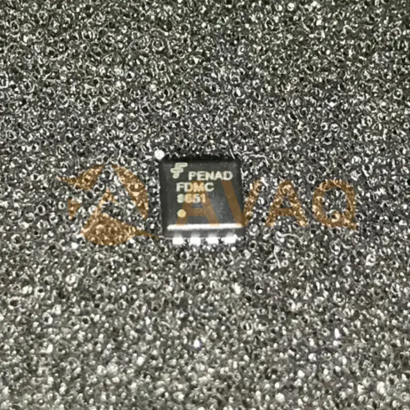
N-Channel Power Trench® MOSFET 30V, 20A, 6.1mΩ
Power33Manufacturer:
Mfr.Part #:
FDMC8651
Datasheet:
Pbfree Code:
Yes
Part Life Cycle Code:
Active
Reach Compliance Code:
compliant
ECCN Code:
EAR99
EDA/CAD Models:
Send all BOMs to ![]() [email protected],
or fill out the form below for a quote on FDMC8651. Guaranteed response within
[email protected],
or fill out the form below for a quote on FDMC8651. Guaranteed response within
![]() 12hr.
12hr.
Please fill in the short form below and we will provide you the quotation immediately.
Elevate the efficiency of your DC/DC converters with the FDMC8651, a groundbreaking device meticulously designed to enhance performance. Through the integration of advanced MOSFET construction techniques, this product offers unparalleled optimization of gate charge and capacitance components, effectively reducing switching losses. With its low gate resistance and minimal Miller charge, the FDMC8651 delivers exceptional performance across adaptive and fixed dead time gate drive circuits. Maintaining a very low rDS(on) capability, this device operates seamlessly at sub logic-levels, making it an ideal choice for applications that demand top-tier efficiency and precision
| Source Content uid | FDMC8651 | Pbfree Code | Yes |
| Part Life Cycle Code | Active | Reach Compliance Code | compliant |
| ECCN Code | EAR99 | Factory Lead Time | 50 Weeks |
| Avalanche Energy Rating (Eas) | 128 mJ | Case Connection | DRAIN |
| Configuration | SINGLE WITH BUILT-IN DIODE | DS Breakdown Voltage-Min | 30 V |
| Drain Current-Max (ID) | 15 A | Drain-source On Resistance-Max | 0.0061 Ω |
| FET Technology | METAL-OXIDE SEMICONDUCTOR | JESD-30 Code | S-PDSO-N5 |
| JESD-609 Code | e4 | Moisture Sensitivity Level | 1 |
| Number of Elements | 1 | Number of Terminals | 5 |
| Operating Mode | ENHANCEMENT MODE | Operating Temperature-Max | 150 °C |
| Operating Temperature-Min | -55 °C | Peak Reflow Temperature (Cel) | NOT SPECIFIED |
| Polarity/Channel Type | N-CHANNEL | Power Dissipation-Max (Abs) | 41 W |
| Pulsed Drain Current-Max (IDM) | 60 A | Qualification Status | Not Qualified |
| Surface Mount | YES | Terminal Finish | Nickel/Palladium (Ni/Pd) |
| Terminal Form | NO LEAD | Terminal Position | DUAL |
| Time@Peak Reflow Temperature-Max (s) | NOT SPECIFIED | Transistor Application | SWITCHING |
| Transistor Element Material | SILICON |
After-Sales & Settlement Related
 Payment
Payment Method


For alternative payment channels, please reach out to us at:
[email protected] Shipping & Packing
Shipping Method


AVAQ determines and packages all devices based on electrostatic discharge (ESD) and moisture sensitivity level (MSL) protection requirements.
 Warranty

365-Day Product
Quality Guarantee
We promise to provide 365 days quality assurance service for all our products.
| Qty. | Unit Price | Ext. Price |
|---|---|---|
| 1+ | $0.812 | $0.81 |
| 10+ | $0.795 | $7.95 |
| 30+ | $0.782 | $23.46 |
| 100+ | $0.770 | $77.00 |
The prices below are for reference only.
