Payment Method


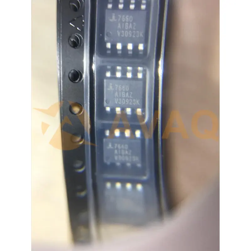
Switching Voltage Regulators W/ANNEAL CMOS VAGE CNVRTR IND
SOIC-8Manufacturer:
Mfr.Part #:
ICL7660AIBAZA
Datasheet:
Pbfree Code:
Yes
Part Life Cycle Code:
Active
Pin Count:
8
Reach Compliance Code:
compliant
EDA/CAD Models:
All bill of materials (BOM) can be sent via email to ![]() [email protected],
or fill below form to Quote for ICL7660AIBAZA, guaranteed quotes back within
[email protected],
or fill below form to Quote for ICL7660AIBAZA, guaranteed quotes back within
![]() 12hr.
12hr.
Please fill in the short form below and we will provide you the quotation immediately.
The ICL7660S and ICL7660A Super Voltage Converters are monolithic CMOS voltage conversion ICs that guarantee significant performance advantages over other similar devices. They are direct replacements for the industry standard ICL7660 offering an extended operating supply voltage range up to 12V, with lower supply current. A Frequency Boost pin has been incorporated to enable the user to achieve lower output impedance despite using smaller capacitors. All improvements are highlighted in the “Electrical Specifications” section on page 3 of the datasheet. Critical parameters are guaranteed over the entire commercial and industrial temperature ranges. The ICL7660S and ICL7660A perform supply voltage conversions from positive to negative for an input range of 1. 5V to 12V, resulting in complementary output voltages of -1. 5V to -12V. Only two non-critical external capacitors are needed, for the charge pump and charge reservoir functions. The ICL7660S and ICL7660A can be connected to function as a voltage doubler and will generate up to 22. 8V with a 12V input. They can also be used as a voltage multipliers or voltage dividers. Each chip contains a series DC power supply regulator, RC oscillator, voltage level translator, and four output power MOS switches. The oscillator, when unloaded, oscillates at a nominal frequency of 10kHz for an input supply voltage of 5. 0V. This frequency can be lowered by the addition of an external capacitor to the “OSC” terminal, or the oscillator may be over-driven by an external clock. The “LV” terminal may be tied to GND to bypass the internal series regulator and improve low voltage (LV) operation. At medium to high voltages (3. 5V to 12V), the LV pin is left floating to prevent device latchup. In some applications, an external Schottky diode from VOUT to CAP- is needed to guarantee latchup free operation (see Do’s and Don’ts section on page 8 of the datasheet).
| Source Content uid | ICL7660AIBAZA | Pbfree Code | Yes |
| Part Life Cycle Code | Active | Pin Count | 8 |
| Reach Compliance Code | compliant | ECCN Code | EAR99 |
| HTS Code | 8542.39.00.01 | Analog IC - Other Type | SWITCHED CAPACITOR CONVERTER |
| JESD-30 Code | R-PDSO-G8 | Moisture Sensitivity Level | 1 |
| Number of Functions | 1 | Number of Terminals | 8 |
| Peak Reflow Temperature (Cel) | 260 | Surface Mount | YES |
| Switcher Configuration | DOUBLER | Technology | CMOS |
| Temperature Grade | INDUSTRIAL | Terminal Finish | MATTE TIN |
| Terminal Form | GULL WING | Terminal Position | DUAL |
| Time@Peak Reflow Temperature-Max (s) | 30 |
After-Sales & Settlement Related
 Payment
Payment Method


For alternative payment channels, please reach out to us at:
[email protected] Shipping & Packing
Shipping Method


AVAQ determines and packages all devices based on electrostatic discharge (ESD) and moisture sensitivity level (MSL) protection requirements.
 Warranty

365-Day Product
Quality Guarantee
We promise to provide 365 days quality assurance service for all our products.
| Qty. | Unit Price | Ext. Price |
|---|---|---|
| 1+ | $1.284 | $1.28 |
| 200+ | $0.497 | $99.40 |
| 500+ | $0.480 | $240.00 |
| 1000+ | $0.470 | $470.00 |
The prices below are for reference only.

ISL88739HRZ
Renesas Technology Corp
975+ $4.077

HIP4082IBZ
Renesas
1000+ $2.447

M51995AFP
Mitsubishi Electric
Efficient voltage mode control for high-speed applications

ISL88739AHRZ
Renesas Technology Corp
Designed for efficient and safe charging of lithium polymer batteries

CA3059
onsemi
Zero voltage regulators
