Payment Method


LCMXO2-2000HC-4FTG256I: 2112 Logic Elements, 207 I/O, 2.5 / 3.3 V Operating Voltage
FTBGA-256Manufacturer:
Mfr.Part #:
LCMXO2-2000HC-4FTG256I
Datasheet:
Series:
LCMXO2
Number Of Logic Elements:
2112 LE
Adaptive Logic Modules - ALMs:
1056 ALM
Embedded Memory:
74 kbit
EDA/CAD Models:
Send all BOMs to ![]() [email protected],
or fill out the form below for a quote on LCMXO2-2000HC-4FTG256I. Guaranteed response within
[email protected],
or fill out the form below for a quote on LCMXO2-2000HC-4FTG256I. Guaranteed response within
![]() 12hr.
12hr.
Please fill in the short form below and we will provide you the quotation immediately.
The LCMXO2-2000HC-4FTG256I, manufactured by Lattice Semiconductor, is a field-programmable gate array (FPGA) with a 2000 LUT capacity and 4000 logic elements. It comes in a 256-pin fine pitch BGA package, making it suitable for compact designs where space is limited. With 112 kbits of embedded memory, 49 I/O pins, and dedicated hardware multipliers and PLLs, this FPGA offers enhanced performance for a wide range of applications. Operating at a maximum speed of 300 MHz and supporting various I/O standards such as LVCMOS, LVTTL, and LVDS, it is well-suited for industrial automation, telecommunications, and consumer electronics. Its low power consumption and high integration capabilities make it a versatile choice for prototyping and product development
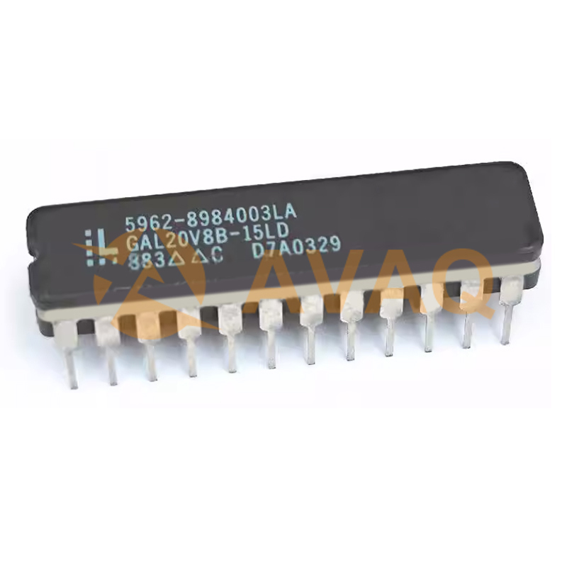
| Product Category | FPGA - Field Programmable Gate Array | Series | LCMXO2 |
| Number of Logic Elements | 2112 LE | Adaptive Logic Modules - ALMs | 1056 ALM |
| Embedded Memory | 74 kbit | Number of I/Os | 206 I/O |
| Supply Voltage - Min | 2.375 V | Supply Voltage - Max | 3.6 V |
| Minimum Operating Temperature | - 40 C | Maximum Operating Temperature | + 100 C |
| Number of Transceivers | - | Mounting Style | SMD/SMT |
| Packaging | [ "Tray" ] | Distributed RAM | 16 kbit |
| Embedded Block RAM - EBR | 74 kbit | Maximum Operating Frequency | 269 MHz |
| Moisture Sensitive | Yes | Number of Logic Array Blocks - LABs | 264 LAB |
| Operating Supply Current | 82 uA | Operating Supply Voltage | 2.5 V/3.3 V |
| Product Type | FPGA - Field Programmable Gate Array | Factory Pack Quantity | 90 |
| Subcategory | Programmable Logic ICs | Total Memory | 170 kbit |
| Tradename | MachXO2 | Unit Weight | 0.098203 oz |
After-Sales & Settlement Related
 Payment
Payment Method


For alternative payment channels, please reach out to us at:
[email protected] Shipping & Packing
Shipping Method


AVAQ determines and packages all devices based on electrostatic discharge (ESD) and moisture sensitivity level (MSL) protection requirements.
 Warranty

365-Day Product
Quality Guarantee
We promise to provide 365 days quality assurance service for all our products.
| Qty. | Unit Price | Ext. Price |
|---|---|---|
| 1+ | $8.100 | $8.10 |
| 10+ | $7.083 | $70.83 |
| 30+ | $6.462 | $193.86 |
| 100+ | $5.943 | $594.30 |
The prices below are for reference only.
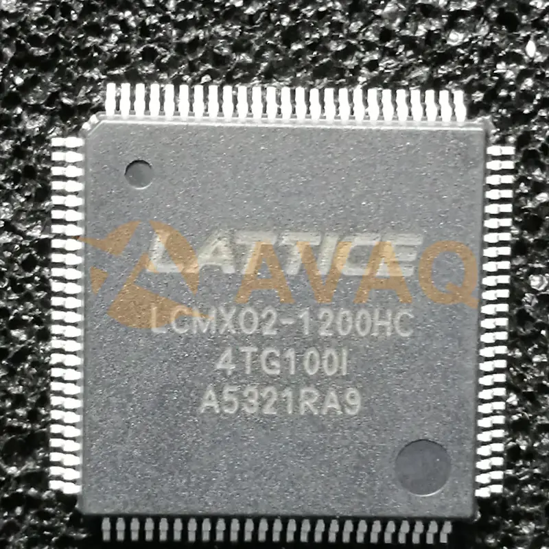
LCMXO2-1200HC-4TG100I
LATTICE
1000+ $3.419
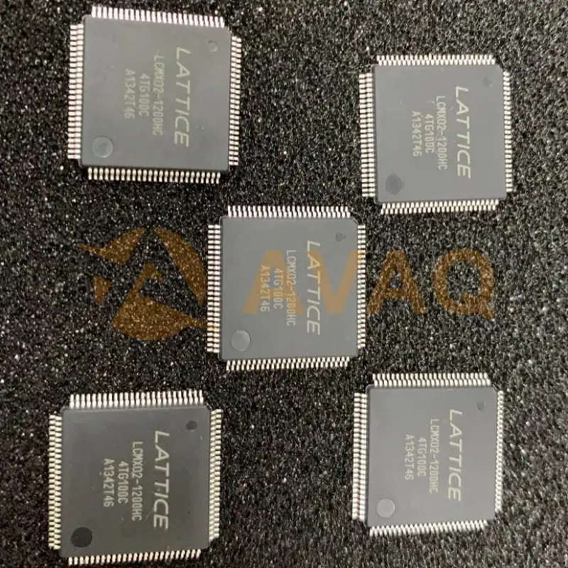
LCMXO2-1200HC-4TG100C
LATTICE
1000+ $2.604

LC4032V-75TN48C
Lattice
High Performance E2 CMOS PLD Generic Array Logic
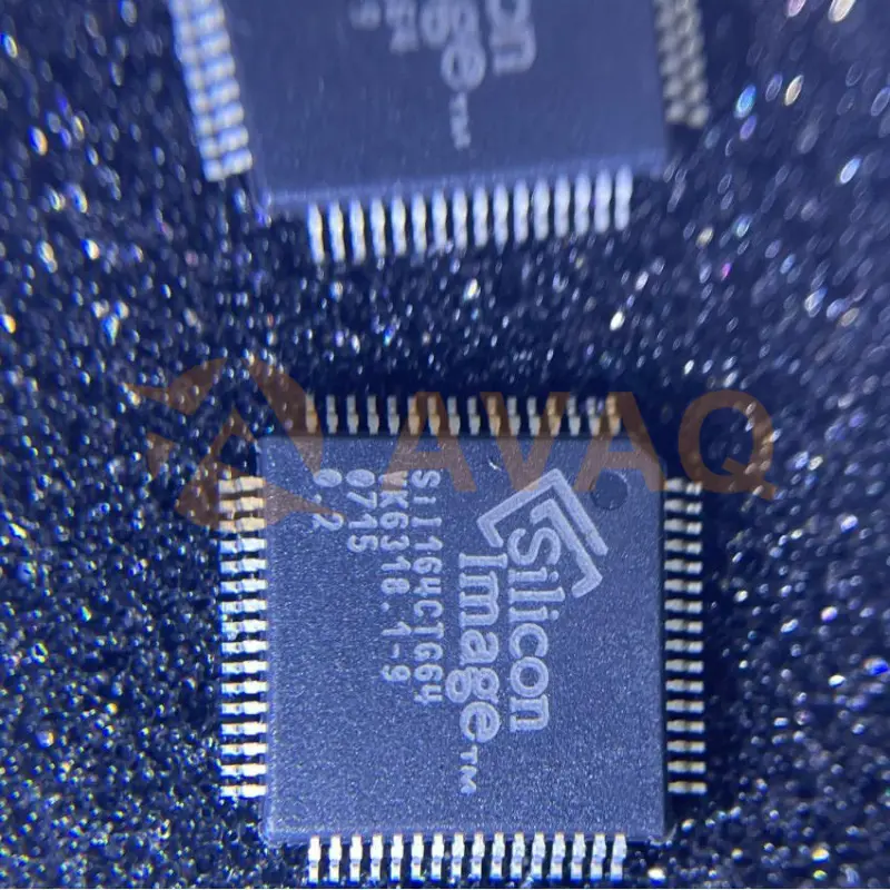
SiI164CTG64
Lattice
TQFP package Transmitter with 2 transmitters
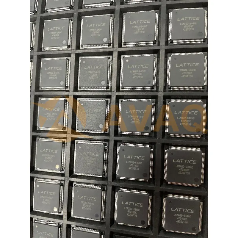
LCMXO2-640HC-4TG100C
Lattice
ROHS Programmable Logic Device (CPLDs/FPGAs) 640 80 TQFP-100(14x14) LCMXO2-640HC-4TG100C