Payment Method


Low noise figure
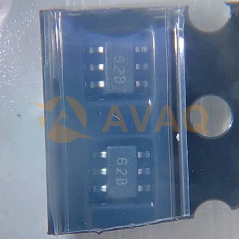
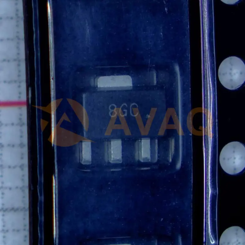
SOT-89-3Manufacturer:
Mfr.Part #:
MGA-30889-BLKG
Datasheet:
Frequency:
40MHz ~ 2.6GHz
P1dB:
20.3dBm
Gain:
15.7dB
Noise Figure:
2dB
EDA/CAD Models:
Send all BOMs to ![]() [email protected],
or fill out the form below for a quote on MGA-30889-BLKG. Guaranteed response within
[email protected],
or fill out the form below for a quote on MGA-30889-BLKG. Guaranteed response within
![]() 12hr.
12hr.
Please fill in the short form below and we will provide you the quotation immediately.
Designed to meet the demands of modern communication and radar systems, the MGA-30889-BLKG boasts a compact and lead-free package that is perfect for space-limited environments. Its outstanding linearity ensures minimal distortion and interference, making it an excellent choice for RF and microwave applications where signal integrity is paramount
| Frequency | 40MHz ~ 2.6GHz | P1dB | 20.3dBm |
| Gain | 15.7dB | Noise Figure | 2dB |
| RF Type | General Purpose | Voltage - Supply | 5V |
| Current - Supply | 65mA | Test Frequency | 1.95GHz |
| Mounting Type | Surface Mount |
After-Sales & Settlement Related
 Payment
Payment Method


For alternative payment channels, please reach out to us at:
[email protected] Shipping & Packing
Shipping Method


AVAQ determines and packages all devices based on electrostatic discharge (ESD) and moisture sensitivity level (MSL) protection requirements.
 Warranty

365-Day Product
Quality Guarantee
We promise to provide 365 days quality assurance service for all our products.
| Qty. | Unit Price | Ext. Price |
|---|---|---|
| 1+ | - | - |
The prices below are for reference only.

BCM43438KUBG
Broadcom
Single-Chip IEEE 802.11ac b/g/n MAC/Baseband/Radio with Integrated Bluetooth 4.1 and FM Receiver

MGA-62563-TR1G
Broadcom Limited
3 Volt RF Amplifier with 22 dB Signal Boost

MGA-81563-TR1G
BROADCOM
Wideband RF amplifier

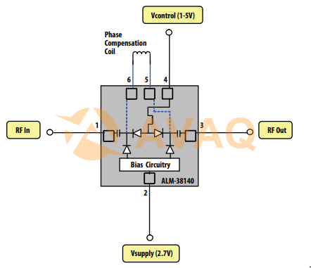
ALM-38140
Broadcom Corporation
Wideband tuning with unparalleled accurac

BCM85110IFSBG
BROADCOM
Compact yet powerful radio frequency technology
