Payment Method


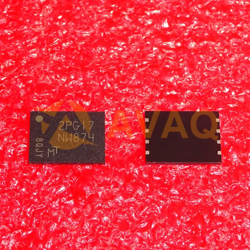
FLASH - NAND Memory IC 2Gbit SPI 8-UPDFN (8x6) (MLP8)
8-UDFNManufacturer:
Micron Technology Inc.
Mfr.Part #:
MT29F2G01ABAGDWB-IT:G TR
Datasheet:
Programmabe:
Not Verified
Memory Type:
Non-Volatile
Memory Format:
FLASH
Technology:
FLASH - NAND
EDA/CAD Models:
All bill of materials (BOM) can be sent via email to ![]() [email protected],
or fill below form to Quote for MT29F2G01ABAGDWB-IT:G TR, guaranteed quotes back within
[email protected],
or fill below form to Quote for MT29F2G01ABAGDWB-IT:G TR, guaranteed quotes back within
![]() 12hr.
12hr.
Please fill in the short form below and we will provide you the quotation immediately.
Utilizing NAND technology, this flash memory chip delivers lightning-fast read and write speeds, making it effortless to store and access large volumes of data. Its compact design ensures compatibility with space-restricted devices without compromising on performance or reliability
| Programmabe | Not Verified | Memory Type | Non-Volatile |
| Memory Format | FLASH | Technology | FLASH - NAND |
| Memory Size | 2Gbit | Memory Organization | 2G x 1 |
| Memory Interface | SPI | Voltage - Supply | 2.7V ~ 3.6V |
| Operating Temperature | -40°C ~ 85°C (TA) | Mounting Type | Surface Mount |
| Base Product Number | MT29F2G01 |
After-Sales & Settlement Related
 Payment
Payment Method


For alternative payment channels, please reach out to us at:
[email protected] Shipping & Packing
Shipping Method


AVAQ determines and packages all devices based on electrostatic discharge (ESD) and moisture sensitivity level (MSL) protection requirements.
 Warranty

365-Day Product
Quality Guarantee
We promise to provide 365 days quality assurance service for all our products.
| Qty. | Unit Price | Ext. Price |
|---|---|---|
| 1+ | - | - |
The prices below are for reference only.
