Payment Method


Microcontroller Units (MCUs/MPUs/SOCs) SAK-XC2224L-20F66V AA VQFN-48-EP(7x7) ROHS
48-VFQFNExposedPadManufacturer:
Infineon Technologies
Mfr.Part #:
SAK-XC2224L-20F66V AA
Datasheet:
Series:
XC22xxL
Programmabe:
Not Verified
Core Processor:
C166SV2
Core Size:
16/32-Bit
EDA/CAD Models:
All bill of materials (BOM) can be sent via email to ![]() [email protected],
or fill below form to Quote for SAK-XC2224L-20F66V AA, guaranteed quotes back within
[email protected],
or fill below form to Quote for SAK-XC2224L-20F66V AA, guaranteed quotes back within
![]() 12hr.
12hr.
Please fill in the short form below and we will provide you the quotation immediately.
Engineered with an array of analog and digital inputs and outputs, the SAK-XC2224L-20F66V AA offers flexibility in configuring input and output settings to cater to diverse project requirements. Furthermore, its built-in safety features, such as voltage monitoring, watchdog timer, and error correction code (ECC) for memory, provide added assurance of reliable operation even in critical scenarios. The MCU's low power consumption and robust design further underscore its suitability for demanding embedded systems that demand optimal performance and unwavering reliability
| Series | XC22xxL | Programmabe | Not Verified |
| Core Processor | C166SV2 | Core Size | 16/32-Bit |
| Speed | 66MHz | Connectivity | CANbus, I²C, LINbus, SPI, SSC, UART/USART, USI |
| Peripherals | I²S, POR, PWM, WDT | Number of I/O | 33 |
| Program Memory Size | 160KB (160K x 8) | Program Memory Type | FLASH |
| RAM Size | 10K x 8 | Voltage - Supply (Vcc/Vdd) | 3V ~ 5.5V |
| Data Converters | A/D 10x12b | Oscillator Type | Internal |
| Operating Temperature | -40°C ~ 125°C (TA) | Mounting Type | Surface Mount |
| Base Product Number | XC2224 |
After-Sales & Settlement Related
 Payment
Payment Method


For alternative payment channels, please reach out to us at:
[email protected] Shipping & Packing
Shipping Method


AVAQ determines and packages all devices based on electrostatic discharge (ESD) and moisture sensitivity level (MSL) protection requirements.
 Warranty

365-Day Product
Quality Guarantee
We promise to provide 365 days quality assurance service for all our products.
| Qty. | Unit Price | Ext. Price |
|---|---|---|
| 1+ | $9.371 | $9.37 |
| 200+ | $3.628 | $725.60 |
| 500+ | $3.499 | $1,749.50 |
| 1000+ | $3.435 | $3,435.00 |
The prices below are for reference only.

C100
Issi
Video ICs 4MP H.265 Video Processor - 64MB DDR2, BGA85, 5mm x 6mm

NE555
Texas Instruments
100kHz operation frequency with low power consumption for long-lasting performance

CD4017
Onsemi
Compact digital counter for precision measurement application

74LS04
Onsemi
High-quality die for professional use only, unsurfaced and untested

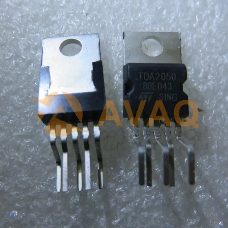
TDA2050
Stmicroelectronics
Effortlessly drives your speakers with crystal-clear sound and robust power