Payment Method


Low-power, low-latency device for modern embedded systems
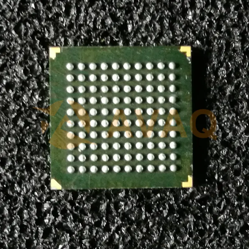
nFBGA-100Manufacturer:
Mfr.Part #:
SCANSTA112SM
Datasheet:
Pbfree Code:
Yes
Part Life Cycle Code:
Active
Pin Count:
100
Reach Compliance Code:
not_compliant
EDA/CAD Models:
Send all BOMs to ![]() [email protected],
or fill out the form below for a quote on SCANSTA112SM. Guaranteed response within
[email protected],
or fill out the form below for a quote on SCANSTA112SM. Guaranteed response within
![]() 12hr.
12hr.
Please fill in the short form below and we will provide you the quotation immediately.
The SCANSTA112 extends the IEEE Std. 1149.1 test bus into a multidrop test bus environment. The advantage of a multidrop approach over a single serial scan chain is improved test throughput and the ability to remove a board from the system and retain test access to the remaining modules. Each SCANSTA112 supports up to 7 local IEEE1149.1 scan chains which can be accessed individually or combined serially.
Addressing is accomplished by loading the instruction register with a value matching that of the Slot inputs. Backplane and inter-board testing can easily be accomplished by parking the local TAP Controllers in one of the stable TAP Controller states via a Park instruction. The 32-bit TCK counter enables built in self test operations to be performed on one port while other scan chains are simultaneously tested.
The STA112 has a unique feature in that the backplane port and the LSP0 port are bidirectional. They can be configured to alternatively act as the master or slave port so an alternate test master can take control of the entire scan chain network from the LSP0 port while the backplane port becomes a slave.
| Source Content uid | SCANSTA112SM | Pbfree Code | Yes |
| Part Life Cycle Code | Active | Pin Count | 100 |
| Reach Compliance Code | not_compliant | ECCN Code | EAR99 |
| HTS Code | 8542.39.00.01 | External Data Bus Width | |
| JESD-30 Code | S-PBGA-B100 | Moisture Sensitivity Level | 3 |
| Number of Terminals | 100 | Peak Reflow Temperature (Cel) | 235 |
| Surface Mount | YES | Technology | CMOS |
| Temperature Grade | INDUSTRIAL | Terminal Finish | Tin/Lead (Sn/Pb) |
| Terminal Form | BALL | Terminal Position | BOTTOM |
| Time@Peak Reflow Temperature-Max (s) | NOT SPECIFIED | uPs/uCs/Peripheral ICs Type | MICROPROCESSOR CIRCUIT |
After-Sales & Settlement Related
 Payment
Payment Method


For alternative payment channels, please reach out to us at:
[email protected] Shipping & Packing
Shipping Method


AVAQ determines and packages all devices based on electrostatic discharge (ESD) and moisture sensitivity level (MSL) protection requirements.
 Warranty

365-Day Product
Quality Guarantee
We promise to provide 365 days quality assurance service for all our products.
| Qty. | Unit Price | Ext. Price |
|---|---|---|
| 1+ | $22.844 | $22.84 |
| 30+ | $21.892 | $656.76 |
The prices below are for reference only.
