Payment Method


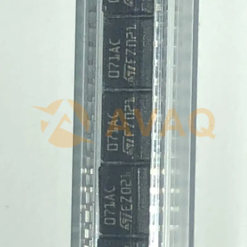
JFET-input operational amplifier with 13-V/µs slew rate
SOIC-8Manufacturer:
Mfr.Part #:
TL071ACD
Datasheet:
Pbfree Code:
Yes
Part Life Cycle Code:
Obsolete
Pin Count:
8
Reach Compliance Code:
compliant
EDA/CAD Models:
Send all BOMs to ![]() [email protected],
or fill out the form below for a quote on TL071ACD. Guaranteed response within
[email protected],
or fill out the form below for a quote on TL071ACD. Guaranteed response within
![]() 12hr.
12hr.
Please fill in the short form below and we will provide you the quotation immediately.
With a focus on precision and reliability, the TL071ACD is a go-to choice for applications that require high accuracy and minimal noise. Its low input bias current and low offset voltage ensure precise operation, while the high slew rate and wide bandwidth make it suitable for high-frequency tasks. Housed in an 8-pin SOIC package, it offers easy integration into various circuit designs, catering to diverse application needs. The wide supply voltage range further enhances its versatility, making it a valuable asset in the realm of operational amplifiers
| Source Content uid | TL071ACD | Pbfree Code | Yes |
| Part Life Cycle Code | Obsolete | Pin Count | 8 |
| Reach Compliance Code | compliant | ECCN Code | EAR99 |
| HTS Code | 8542.33.00.01 | Amplifier Type | OPERATIONAL AMPLIFIER |
| Architecture | VOLTAGE-FEEDBACK | Average Bias Current-Max (IIB) | 0.007 µA |
| Bias Current-Max (IIB) @25C | 0.0002 µA | Common-mode Reject Ratio-Min | 75 dB |
| Common-mode Reject Ratio-Nom | 100 dB | Frequency Compensation | YES |
| Input Offset Current-Max (IIO) | 0.002 µA | Input Offset Voltage-Max | 6000 µV |
| JESD-30 Code | R-PDSO-G8 | JESD-609 Code | e4 |
| Length | 4.9 mm | Low-Bias | YES |
| Low-Offset | NO | Micropower | NO |
| Moisture Sensitivity Level | 1 | Neg Supply Voltage Limit-Max | -18 V |
| Neg Supply Voltage-Nom (Vsup) | -15 V | Number of Functions | 1 |
| Number of Terminals | 8 | Operating Temperature-Max | 70 °C |
| Operating Temperature-Min | Packing Method | TUBE | |
| Peak Reflow Temperature (Cel) | 260 | Power | NO |
| Programmable Power | NO | Qualification Status | Not Qualified |
| Seated Height-Max | 1.75 mm | Slew Rate-Min | 8 V/us |
| Slew Rate-Nom | 13 V/us | Supply Current-Max | 2.5 mA |
| Supply Voltage Limit-Max | 18 V | Supply Voltage-Nom (Vsup) | 15 V |
| Surface Mount | YES | Technology | BIPOLAR |
| Temperature Grade | COMMERCIAL | Terminal Finish | Nickel/Palladium/Gold (Ni/Pd/Au) |
| Terminal Form | GULL WING | Terminal Pitch | 1.27 mm |
| Terminal Position | DUAL | Time@Peak Reflow Temperature-Max (s) | NOT SPECIFIED |
| Unity Gain BW-Nom | 3000 | Voltage Gain-Min | 25000 |
| Wideband | NO | Width | 3.9 mm |
After-Sales & Settlement Related
 Payment
Payment Method


For alternative payment channels, please reach out to us at:
[email protected] Shipping & Packing
Shipping Method


AVAQ determines and packages all devices based on electrostatic discharge (ESD) and moisture sensitivity level (MSL) protection requirements.
 Warranty

365-Day Product
Quality Guarantee
We promise to provide 365 days quality assurance service for all our products.
| Qty. | Unit Price | Ext. Price |
|---|---|---|
| 1+ | $3.460 | $3.46 |
| 200+ | $1.340 | $268.00 |
| 500+ | $1.292 | $646.00 |
| 1000+ | $1.269 | $1,269.00 |
The prices below are for reference only.
