Payment Method


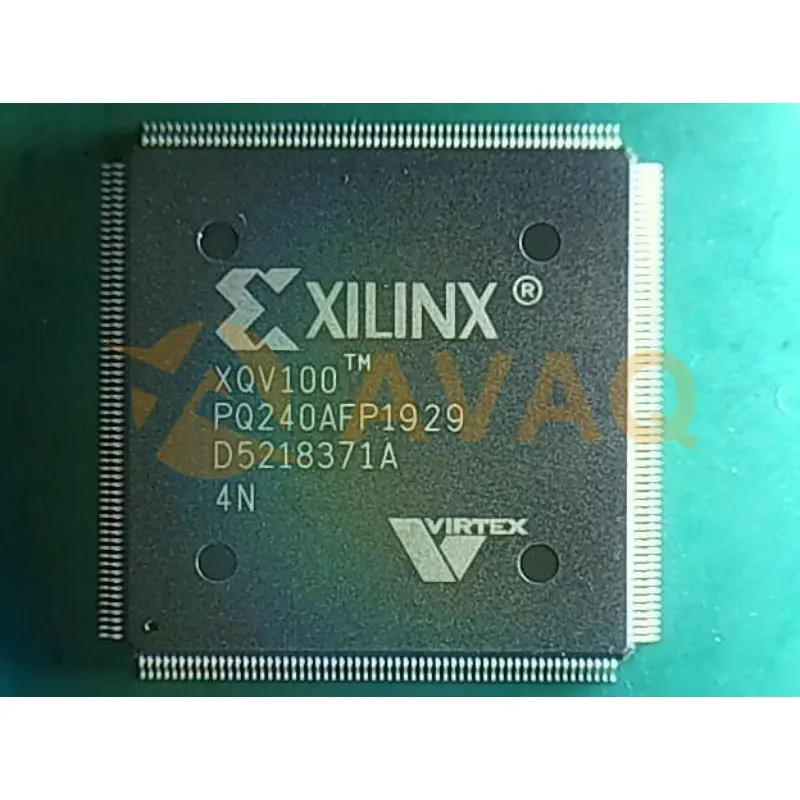
IC FPGA QPRO VIRTEX 240-PQFP
QFP240Manufacturer:
Mfr.Part #:
XQV100-4PQ240N
Datasheet:
ECCN (US):
EAR99
HTS:
8541.29.00.95
Automotive:
No
PPAP:
No
EDA/CAD Models:
Send all BOMs to ![]() [email protected],
or fill out the form below for a quote on XQV100-4PQ240N. Guaranteed response within
[email protected],
or fill out the form below for a quote on XQV100-4PQ240N. Guaranteed response within
![]() 12hr.
12hr.
Please fill in the short form below and we will provide you the quotation immediately.
| ECCN (US) | EAR99 | Part Status | Unconfirmed |
| HTS | 8541.29.00.95 | Automotive | No |
| PPAP | No | Category | Power MOSFET |
| Configuration | Single | Channel Mode | Enhancement |
| Channel Type | N | Number of Elements per Chip | 1 |
| Maximum Drain Source Voltage (V) | 600 | Maximum Gate Source Voltage (V) | ±30 |
| Maximum Gate Threshold Voltage (V) | 4 | Maximum Continuous Drain Current (A) | 33 |
| Maximum Gate Source Leakage Current (nA) | 100 | Maximum IDSS (uA) | 1 |
| Maximum Drain Source Resistance (mOhm) | 99@10V | Typical Gate Charge @ Vgs (nC) | 100@10V |
| Typical Gate Charge @ 10V (nC) | 100 | Typical Input Capacitance @ Vds (pF) | 3508@100V |
| Maximum Power Dissipation (mW) | 278000 | Typical Fall Time (ns) | 54 |
| Typical Rise Time (ns) | 60 | Typical Turn-Off Delay Time (ns) | 99 |
| Typical Turn-On Delay Time (ns) | 28 | Minimum Operating Temperature (°C) | -55 |
| Maximum Operating Temperature (°C) | 150 | Mounting | Through Hole |
| PCB changed | 3 | Tab | Tab |
| Pin Count | 3 | Lead Shape | Through Hole |
After-Sales & Settlement Related
 Payment
Payment Method


For alternative payment channels, please reach out to us at:
[email protected] Shipping & Packing
Shipping Method


AVAQ determines and packages all devices based on electrostatic discharge (ESD) and moisture sensitivity level (MSL) protection requirements.
 Warranty

365-Day Product
Quality Guarantee
We promise to provide 365 days quality assurance service for all our products.
| Qty. | Unit Price | Ext. Price |
|---|---|---|
| 1+ | - | - |
The prices below are for reference only.
