Payment Method


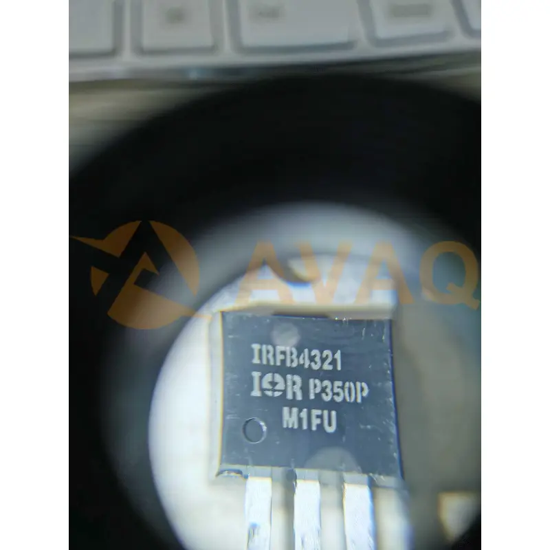
The IRFB4321PBF is a high-power N-channel MOSFET designed to handle up to 150 volts and 83 amperes, presented in a TO-220AB package
TO-220-3Manufacturer:
Mfr.Part #:
IRFB4321PBF
Datasheet:
Part Life Cycle Code:
Active
Reach Compliance Code:
compliant
ECCN Code:
EAR99
Factory Lead Time:
65 Weeks
EDA/CAD Models:
Send all BOMs to ![]() [email protected],
or fill out the form below for a quote on IRFB4321PBF. Guaranteed response within
[email protected],
or fill out the form below for a quote on IRFB4321PBF. Guaranteed response within
![]() 12hr.
12hr.
Please fill in the short form below and we will provide you the quotation immediately.
The IRFB4321PBF Power Field-Effect Transistor is a high-quality, high-performance component designed for demanding power applications. With a 75A maximum current rating and 150V voltage rating, this N-Channel MOSFET offers reliable and efficient power handling. The low on-resistance of 0.015ohm ensures minimal power loss and optimal energy efficiency. Housed in a TO-220AB package with lead-free, plastic construction, the IRFB4321PBF provides excellent thermal performance and complies with environmental standards. Whether used in motor controls, solar inverters, or welding equipment, this transistor delivers exceptional performance and rugged reliability
| Source Content uid | IRFB4321PBF | Part Life Cycle Code | Active |
| Reach Compliance Code | compliant | ECCN Code | EAR99 |
| Factory Lead Time | 65 Weeks | Avalanche Energy Rating (Eas) | 120 mJ |
| Case Connection | DRAIN | Configuration | SINGLE WITH BUILT-IN DIODE |
| DS Breakdown Voltage-Min | 150 V | Drain Current-Max (ID) | 75 A |
| Drain-source On Resistance-Max | 0.015 Ω | FET Technology | METAL-OXIDE SEMICONDUCTOR |
| JEDEC-95 Code | TO-220AB | JESD-30 Code | R-PSFM-T3 |
| JESD-609 Code | e3 | Number of Elements | 1 |
| Number of Terminals | 3 | Operating Mode | ENHANCEMENT MODE |
| Operating Temperature-Max | 175 °C | Peak Reflow Temperature (Cel) | 250 |
| Polarity/Channel Type | N-CHANNEL | Power Dissipation-Max (Abs) | 330 W |
| Pulsed Drain Current-Max (IDM) | 330 A | Qualification Status | Not Qualified |
| Surface Mount | NO | Terminal Finish | MATTE TIN OVER NICKEL |
| Terminal Form | THROUGH-HOLE | Terminal Position | SINGLE |
| Time@Peak Reflow Temperature-Max (s) | 30 | Transistor Application | SWITCHING |
| Transistor Element Material | SILICON |
After-Sales & Settlement Related
 Payment
Payment Method


For alternative payment channels, please reach out to us at:
[email protected] Shipping & Packing
Shipping Method


AVAQ determines and packages all devices based on electrostatic discharge (ESD) and moisture sensitivity level (MSL) protection requirements.
 Warranty

365-Day Product
Quality Guarantee
We promise to provide 365 days quality assurance service for all our products.
| Qty. | Unit Price | Ext. Price |
|---|---|---|
| 1+ | $1.925 | $1.92 |
| 10+ | $1.673 | $16.73 |
| 50+ | $1.345 | $67.25 |
| 100+ | $1.184 | $118.40 |
| 600+ | $1.111 | $666.60 |
| 900+ | $1.209 | $1,088.10 |
The prices below are for reference only.
