Payment Method


Ignition Buffer, Regulator PMIC 17-PDBS
ZIP-17Manufacturer:
Mfr.Part #:
TDA3681JR/N2S
Datasheet:
Description:
Multiple voltage regulator with switch and ignition buffer
Number Of Pins:
17
EDA/CAD Models:
Send all BOMs to ![]() [email protected],
or fill out the form below for a quote on TDA3681JR/N2S. Guaranteed response within
[email protected],
or fill out the form below for a quote on TDA3681JR/N2S. Guaranteed response within
![]() 12hr.
12hr.
Please fill in the short form below and we will provide you the quotation immediately.
Ignition Buffer, Regulator PMIC 17-PDBS
| Security Status | COMPANY PUBLIC | Description | Multiple voltage regulator with switch and ignition buffer |
| Number of pins | 17 |
After-Sales & Settlement Related
 Payment
Payment Method


For alternative payment channels, please reach out to us at:
[email protected] Shipping & Packing
Shipping Method


AVAQ determines and packages all devices based on electrostatic discharge (ESD) and moisture sensitivity level (MSL) protection requirements.
 Warranty

365-Day Product
Quality Guarantee
We promise to provide 365 days quality assurance service for all our products.
| Qty. | Unit Price | Ext. Price |
|---|---|---|
| 1+ | - | - |
The prices below are for reference only.

PCA9685PW
Nxp
PCA9685PW Product Description
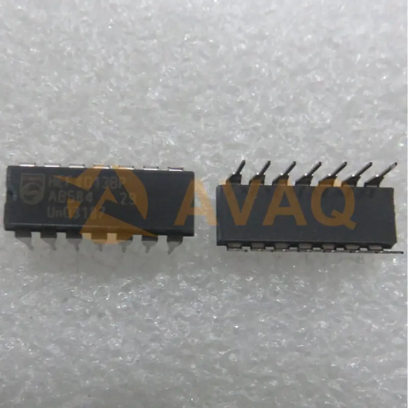
HEF4013BP
Nxp
4000/14000/40000 SERIES DUAL POSITIVE EDGE TRIGGERED D FLIP-FLOP COMPLEMENTARY OUTPUT PDIP14
BU508DF
NXP
onsemi
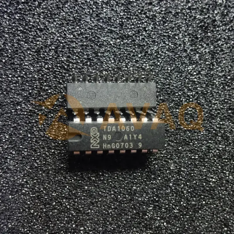
TDA1060
NXP
**Robust System Protection**: With integrated overvoltage

UBA2071AT
Nxp
Achieve optimal CCFL performance with this versatile and accurate control I

