Payment Method


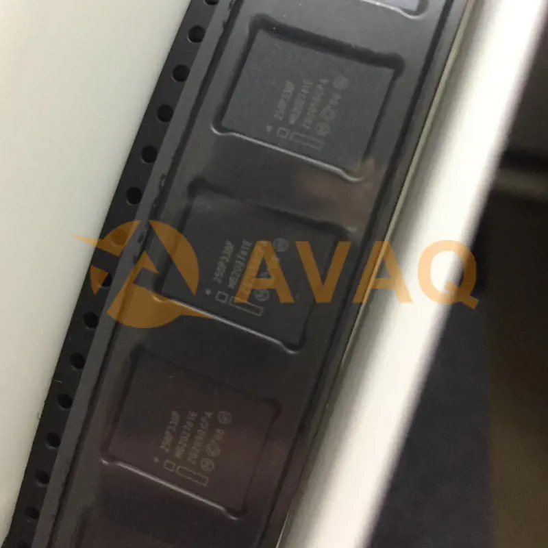
PBGA64-packaged flash memory chip, organized as 16 megabytes by 16 bits, featuring a 95 nanosecond access time
BGA-64Manufacturer:
Alliance Memory, Inc.
Mfr.Part #:
PC28F256P33BFE
Datasheet:
Part Life Cycle Code:
Obsolete
Reach Compliance Code:
compliant
ECCN Code:
EAR99
HTS Code:
8542.32.00.51
EDA/CAD Models:
Send all BOMs to ![]() [email protected],
or fill out the form below for a quote on PC28F256P33BFE. Guaranteed response within
[email protected],
or fill out the form below for a quote on PC28F256P33BFE. Guaranteed response within
![]() 12hr.
12hr.
Please fill in the short form below and we will provide you the quotation immediately.
The PC28F256P33BFE from Microchip Technology is a trustworthy choice for a wide variety of applications. With its voltage range of 2.7V to 3.6V and fast access time of 70ns, it offers reliable performance in industrial automation, automotive, telecommunications, and consumer electronics. Its symmetrical block architecture and integrated Command Set Algorithm provide flexible data storage and enhanced error correction and detection capabilities. Additionally, it boasts high reliability, endurance, and data retention, making it a durable option for your memory needs
| Part Life Cycle Code | Obsolete | Reach Compliance Code | compliant |
| ECCN Code | EAR99 | HTS Code | 8542.32.00.51 |
| Access Time-Max | 95 ns | Additional Feature | BOTTOM BOOT BLOCK, SYNCHRONOUS BURST MODE OPERATION ALSO AVAILABLE |
| Boot Block | BOTTOM | Command User Interface | YES |
| Common Flash Interface | YES | Data Polling | NO |
| JESD-30 Code | R-PBGA-B64 | JESD-609 Code | e1 |
| Length | 13 mm | Memory Density | 268435456 bit |
| Memory IC Type | FLASH | Memory Width | 16 |
| Number of Functions | 1 | Number of Sectors/Size | 4,255 |
| Number of Terminals | 64 | Number of Words | 16777216 words |
| Number of Words Code | 16000000 | Operating Mode | SYNCHRONOUS |
| Operating Temperature-Max | 85 °C | Operating Temperature-Min | -40 °C |
| Organization | 16MX16 | Parallel/Serial | PARALLEL |
| Programming Voltage | 3 V | Qualification Status | Not Qualified |
| Seated Height-Max | 1.2 mm | Sector Size | 16K,64K |
| Standby Current-Max | 0.00021 A | Supply Current-Max | 0.031 mA |
| Supply Voltage-Max (Vsup) | 3.6 V | Supply Voltage-Min (Vsup) | 2.3 V |
| Supply Voltage-Nom (Vsup) | 3 V | Surface Mount | YES |
| Technology | CMOS | Temperature Grade | INDUSTRIAL |
| Terminal Finish | TIN SILVER COPPER | Terminal Form | BALL |
| Terminal Pitch | 1 mm | Terminal Position | BOTTOM |
| Toggle Bit | NO | Type | NOR TYPE |
| Width | 10 mm | Product Category | NOR Flash |
| Mounting Style | SMD/SMT | Series | P33 |
| Memory Size | 256 Mbit | Supply Voltage - Min | 2.3 V |
| Supply Voltage - Max | 3.6 V | Active Read Current - Max | 50 mA |
| Interface Type | Parallel | Maximum Clock Frequency | 52 MHz |
| Data Bus Width | 16 bit | Timing Type | Asynchronous, Synchronous |
| Minimum Operating Temperature | - 40 C | Maximum Operating Temperature | + 85 C |
| Memory Type | NOR | Product Type | NOR Flash |
| Speed | 95 ns | Standard | Common Flash Interface (CFI) |
| Factory Pack Quantity | 864 | Subcategory | Memory & Data Storage |
After-Sales & Settlement Related
 Payment
Payment Method


For alternative payment channels, please reach out to us at:
[email protected] Shipping & Packing
Shipping Method


AVAQ determines and packages all devices based on electrostatic discharge (ESD) and moisture sensitivity level (MSL) protection requirements.
 Warranty

365-Day Product
Quality Guarantee
We promise to provide 365 days quality assurance service for all our products.
| Qty. | Unit Price | Ext. Price |
|---|---|---|
| 1+ | $17.350 | $17.35 |
| 300+ | $6.924 | $2,077.20 |
| 600+ | $6.692 | $4,015.20 |
| 900+ | $6.578 | $5,920.20 |
The prices below are for reference only.
