Payment Method


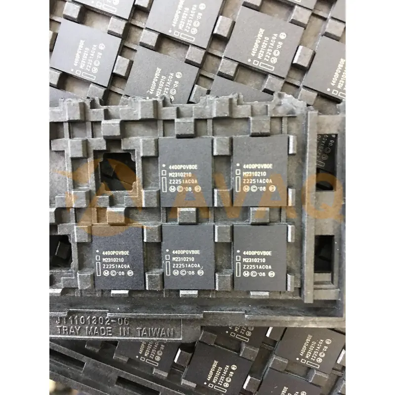
NOR Flash memory for EASYBGA-64(10x13) PC boards
64-EasyBGA (10x13)Manufacturer:
Micron Technology Inc.
Mfr.Part #:
PC48F4400P0VB0EA
Datasheet:
Programmabe:
Not Verified
Memory Type:
Non-Volatile
Memory Format:
FLASH
Technology:
FLASH - NOR
EDA/CAD Models:
All bill of materials (BOM) can be sent via email to ![]() [email protected],
or fill below form to Quote for PC48F4400P0VB0EA, guaranteed quotes back within
[email protected],
or fill below form to Quote for PC48F4400P0VB0EA, guaranteed quotes back within
![]() 12hr.
12hr.
Please fill in the short form below and we will provide you the quotation immediately.
Intel's PC48F4400P0VB0EA NAND Flash memory chip is a powerhouse designed for demanding industrial and embedded systems. Featuring fast data transfer rates through its parallel interface, this chip operates at a supply voltage of 3.3 volts, delivering consistent performance. With error correction and wear leveling capabilities, data integrity is guaranteed, making it a dependable choice for high-speed data storage needs. Its compatibility with various protocols and commands simplifies integration, while its compact form factor and wide operating temperature range enhance its versatility
| Programmabe | Not Verified | Memory Type | Non-Volatile |
| Memory Format | FLASH | Technology | FLASH - NOR |
| Memory Size | 512Mbit | Memory Organization | 32M x 16 |
| Memory Interface | Parallel | Clock Frequency | 52 MHz |
| Write Cycle Time - Word, Page | 100ns | Access Time | 100 ns |
| Voltage - Supply | 1.7V ~ 2V | Operating Temperature | -40°C ~ 85°C (TC) |
| Mounting Type | Surface Mount |
After-Sales & Settlement Related
 Payment
Payment Method


For alternative payment channels, please reach out to us at:
[email protected] Shipping & Packing
Shipping Method


AVAQ determines and packages all devices based on electrostatic discharge (ESD) and moisture sensitivity level (MSL) protection requirements.
 Warranty

365-Day Product
Quality Guarantee
We promise to provide 365 days quality assurance service for all our products.
| Qty. | Unit Price | Ext. Price |
|---|---|---|
| 1+ | $35.983 | $35.98 |
| 200+ | $14.358 | $2,871.60 |
| 500+ | $13.878 | $6,939.00 |
| 864+ | $13.641 | $11,785.82 |
The prices below are for reference only.
